|
in today’s mobile handset market the trend is to provide high performance, low cost components with integration of functionality and small form factor. the ever increasing demand of handset makers to provide smaller, thinner and lower cost packaging solution drives the packaging industry to develop packages that integrates more devices in the same footprint in which devices are integrated within the package in vertical direction, named 3d packaging. in this, the logic device and memory devices are packaged and tested together and then stacked together in a package form typically known as package on packages (pop) technology which is popular and widely used in mobile phone industry.
the pop approach is limited by the fact that the connection between packages is made with solder balls at the periphery of top package to the top of bottom package making the package thicker and taller than an equivalent stack. the pop can be made thinner by reducing the substrate thickness but it leads to package warpage problems. the new generation of stacked packages called fan in package on package (fipop) addresses the limitation posed by pop of increased size and thickness. in fipop package, the connection between top and bottom packages is made by means of a center ball array instead of peripheral ball array. this allows reduction in top package size [1]. the connection to the bottom package is provided by means of wire bonds which allow the bottom package to be smaller. the fipop allows the use of thinner substrate to reduce height without warpage.
fipop structure:
the exposed interconnect land array on top centre surface of bottom package in fipop which is different than conventional pop package having interconnect land array at the top periphery allows the top interconnect array to “fanned–in” towards the centre of the bottom package, thus named as “fanned-in” pop to differentiate with conventional pop typically called “ fanned-out” interconnect array.

figure 1. fipop internal structure [1]
figure 1 is the detailed view of fipop structure and shows interposer substrate connected to the bottom package to allow interconnect to the top package. the interposer substrate is a thin laminated packaging substrate which is mounted on the top of the bottom package using similar manufacturing process and material used in conventional packaging. this interposer is electrically connected to the base package using wire bonds at the periphery. the terminal from the top package is routed to the edge of the interposer, connected to the base substrate by wire bonds and then routed to interconnect with the device mounted to the base substrate and routed to a terminal on the bottom of the package. the wire bond interconnect helps to reduce the package size as the wire bond interconnect at the periphery is much denser than the solder ball interconnect used for conventional pop. decreasing the package size in fipop makes it competitive as compared to conventional pop.
the top central land pattern used in fipop allows using more conventional centre ball grid array package on top. in conventional pop, top package needs to be of the same size or larger than the bottom package to enable the peripheral ball interconnect. the fipop allows decoupling bottom package size with top package thereby use of smaller top memory package is possible [1]. even an “off the shelf” top package such as fbga can be mounted on the top of the fipop but use of such standard packages does not satisfy the minimum size and thickness requirement as desired by mobile electronic industry and customized thin top fbga’s with minimized size, height are developed to suit the industry requirement.
the fipop offers smaller top and bottom package size which is the key consideration for package required in mobile phone applications. the stacked pop is the thickest package which is not suitable to current and future phone industry requirement where minimum size and thickness is critical. even though the fipop package has interposer substrate added on the top of the bottom package, the equivalent or lower stack up height as compared to conventional pop can be achieved by using a thinner base substrate and by minimizing the top to bottom package gap [1]. figure 2 shows comparison of typical pop and fipop stack up height.
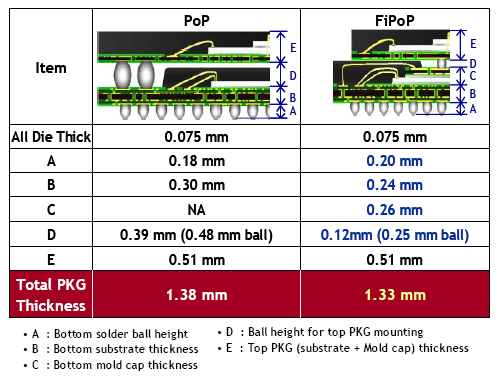
figure 2. fipop and pop stack up height comparison [1]
this achievement is possible due to better co-planarity, flatness and having less warpage during reflow process. for conventional pop package to achieve the acceptable flatness requires thicker base substrate. this is because the periphery of the pop is not covered by encapsulant mold compound (emc) and therefore more susceptible for warpage during reflow process. in fipop, the emc extends to the edge of the package allowing thinner base substrate without excessive warpage. flatness control of the fipop is the key factor for reducing the stacked height.
thermal design considerations:
with reduced package size and improved package performance, thermal management of 3d stack package poses great challenge to thermal engineers even with moderate power consumptions. because of size and cost constraint, external cooling solutions such as heat sink and fan are not recommended for mobile phone thermal management and it is a challenge for this industry and package manufacturers to find a way to dissipate the heat effectively without external cooling methods.
providing a thermal path for heat dissipation is the only option to maintain the junction temperature that meets the thermal requirements of the device. in a typical package construction there are two ways to dissipate the heat from junction to ambient. one is through conduction from die via substrate and then from solder balls to pcb. the heat from pcb is dissipated to ambient via convection/radiation. the second mode is conduction from silicon die via mold compound to the top of the package and then heat is dissipated to ambient via convection/radiation from this surface. previous studies suggest that because of small surface area, very little heat is transferred to ambient from the package top surface.
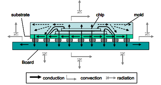
figure 3. heat flow path from die to ambient [2]
figure 3 shows heat dissipation paths in a typical stacked package. the dotted lines are the less efficient thermal paths from die to molding compound to ambient [2]. the solid lines shows efficient heat flow path from die to ambient through the substrate, solder balls and the pcb routing.
for stacked packages there are many factors affecting the thermal performance, but the primary factors can be grouped into three main categories: geometry, material and environment. the stack up geometry and material are related to the package internal thermal design while the environmental category is related to factors outside the package such as handset size, pcb design, parts, etc. in early design studies of packaging, it will be difficult to predict system-level design impact due to wide variety of customer handset designs. in the material category itself the selections are restricted primarily by moisture sensitivity requirements and cost, resulting in a limited choice for material selection impacting thermal performance.
effect of package parameters on fipop thermal performance:
cher bai et al. [2] studied the effect of package parameter on thermal performance of chip scale package (csp) and the study suggests the die size and solder ball i/o pattern have the most impact on package thermal performance.
nagedrappa et al. [3] further implemented the findings from [2] to thermally investigate in detail the impact of package parameter on performance of fipop and studied the effect of three variables: die size, solder ball i/o pattern and number of thermal vias. the following higlights the results of finding by nagedrappa et al.
number of thermal vias:
in fipop, vias are used for routing of signals from bond finger to solder balls through substrate. thermal vias can be added to improve conduction. a rectangular via pattern created under die footprint is studied [3]. the effect of via pattern without solder ball is studied for 24, 29, 34, 39, 44 and 49 vias. each via has 100micron drill diameter and 10 micron plating thickness. the vias were placed under bottom package only and thermal performance of package was tested for top die loading and bottom die loading.
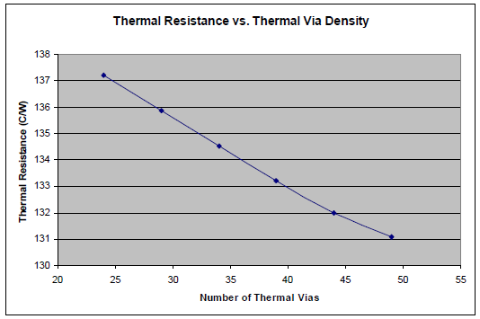
figure 4. effect of thermal via density on thermal resistance [3]
figure 4 shows the behaviour of thermal performance of the package under varying via numbers. there is a small reduction in thermal performance of fipop when thermal vias are added alone [3]. when top die was loaded only, 0.5% improvement was seen with 104% increase in via density. this implies that thermal vias added to the bottom package have little impact on top package thermal performance.
solder ball i/o density:
in fipop package configuration solder balls are used for i/o signals. an increase in number of solder balls are expected to improve thermal performance. the detailed study was carried out by adding extra solder balls to the thermal vias under the die foot print. along with baseline solder ball configuration additional 5, 10, 15, 20 and 25 extra solder balls are added to the thermal vias [3].
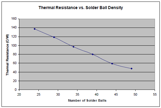
figure 5. effect of solder ball density on thermal resistance [3]
figure 5 shows the effect of solder balls on the thermal performance of fipop. the addition of solder balls at the bottom package has significantly improved package thermal performance. also the results indicate that adding thermal vias without solder ball is ineffective and solder ball must be added along with thermal vias to improve the package thermal performance [3].
die size variation:
the effect of die size on thermal performance of fipop package was studied for 81, 72.9 , 64.8 and 56.7 mm2 [3]. to understand the impact of die size irrespective of thermal vias or solder ball, no thermal vias or solder balls were added directly under the die area.
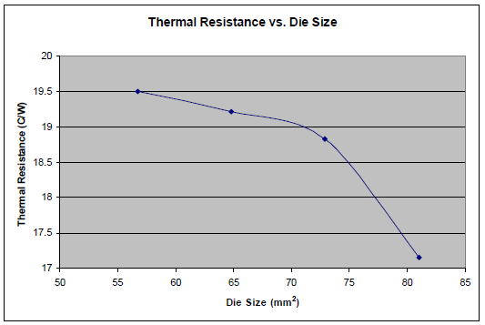
figure 6: effect of solder ball density on thermal resistance [3]
figure 6 shows that smaller the die size higher the package thermal resistance and is contributed to higher heat flux and increased spreading resistance. for bottom die loaded cases, 10% increase in die area results in 2.8% improvement in thermal resistance of the package. in top package loading case, 10% increase in die area results in 8.7% improvement in package thermal resistance.
from the previous studies, it is shown that fipop package thermal resistance decreases with increase in thermal vias and solder balls [3]. it is also shown that thermal vias alone cannot help improve thermal resistance significantly. however addition of solder ball provides significant improvement in package thermal performance. consequently the die size has significant impact on thermal performance and package thermal resistance decreases with the increase in die size.
references
- 1. carson, f., lee,. s, yoon, s. “the development of the fan-in package-on-package”. paper presented at the 2008 58th electronic components and technology conference, 956-63.-2008
- 2. bai, c., and veatch, m. “chip scale package design for thermal performance in mobile handsets”. paper presented at the 2007 electronic components and technology conference, 1415-19-2007
- 3. nagendrappa., n, okamoto.,o, and barez., f,. “thermal characterization of fan-in package-on-packages”. paper presented at the 26th ieee semiconductor thermal measurement & management symposium – 2010
|