|
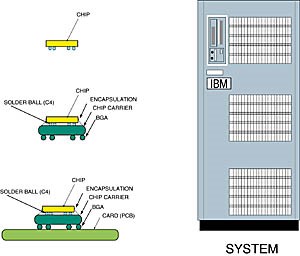
fig. 1: levels in a computer environment.
introduction
increasing demands for higher performance in microprocessors have a direct effect on chip power and heat generation. increased function and miniaturization of the packages result in thermal challenges that require a thorough understanding of the system's thermal performance under all possible field conditions. regardless of the magnitude of the power dissipated by the chip (die), a cooler die means better performance (especially in the cmos technology), increased die reliability and improved package longevity due to a reduction in thermo-mechanical stresses in the package.
in this paper, an overview of the cooling requirements and highlights from the die to the system level will be presented. the interaction of the module level with the system level will be considered in detail via the example of the ibm tape ball grid array (tbga) package. even though the example is that of the tape ball grid array, any other package such as the pbga (plastic ball grid array) or the cbga (ceramic ball grid array) could be used to illustrate and elucidate the concepts.
numerical as well as experimental data on the thermal performance of the tbga package will be used to illustrate the interaction of the module level with the system level cooling. it is also the intention of the paper to show how commonly-used parameters and tests for comparing different packages could lead to misinformation, and that finally the performance of the package and the chip in the system is the most relevant parameter upon which a designer should focus.
figure 1 shows the different levels in the computer system, such as the chip, the module (package), the board and the system. the cooling/heat transfer considerations at each level are unique and are described as follows. at the chip level, heat transfer is by conduction. the thermal resistance (henceforth referred to as the resistance alone) from the junction to the chip is of importance. although the temperature rise from the junction to the chip is usually not too large, it cannot be neglected in some very high powered chips. at the first (module/package) level, again the mechanism is mainly conduction of heat in solids.
the important considerations at this level are the chip/module power dissipation and the module construction - its geometry and material properties. depending on the complexity of the package and the boundary conditions at the boundary of the package; the solution techniques for characterizing thermal performance could range from analytical closed form solutions, solutions of a simple resistance network using the electrical/thermal analog, to numerical (finite difference/finite element) methods.
at the second level (card/board level), the heat transfer mechanism is mainly by convection. the thermal considerations are component (package) geometry and location on the board, flow type (laminar or turbulent) and flow rate, flow distribution and package flow impedance. the governing equations (navier stokes) are non-linear and simple solutions are not amenable. either cfd (computational fluid dynamics) or empirical correlations must be used.
the system level considerations are the ambient environment, namely the temperature, altitude and humidity; blower/fan/pump selection considerations such as capacity, physical size, acoustic noise and location in the machine; and human factors such as acoustic noise, casing temperature and grill locations. the heat transfer analysis is typically restricted to a simple energy balance at this level.
it can be seen that the considerations at different levels are quite different and varied, yet there is considerable interaction between the various levels. as an example, system level considerations determine the air-flow near a component or a board thus affecting heat transfer boundary condition at the board or module level. this in turn affects the chip thermal performance.
for an overview of thermal management in electronic packages, the reader is referred to andros and sammakia (ref. 1) and bar-cohen and kraus (ref. 2). to predict the junction temperature of electronic component packages it has been customary to use a simple equation to calculate the temperature. while the use of the equation is straight-forward, estimating the values of the variables can range from textbook calculations, to computer model simulation, to experimental measurements and requires an expert in the field of heat transfer/fluid flow.
as mentioned earlier, the goal is to achieve a cooler chip junction. for cmos technology, the die performance and reliability is directly dependent upon the die junction temperature, which must be kept below a certain limit. it is therefore extremely important to understand how to estimate the junction temperature of the die and understand the factors at different levels that affect it.
junction temperature prediction
the chip junction temperature in an actual computer environment can be predicted using:
| tj = tambient + dtairheating + dtcase-air +dtj-case |
(1) |
this equation states that the junction temperature rise above ambient temperature comprises the rise due to air heat-up, rise from the local bulk air near the heat sink base or module case (when there is no heat sink) to the heat sink base or module case, respectively (dtcase-air); and the rise from the heat sink base or module case to the junction of the chip (dt j-case). the air heat-up can be caused by heated upstream components and/or the power dissipated by the air-moving device.
the temperature rise from the local air to the module case depends on the convection boundary layer which is a comprehensive heat transfer/fluid flow topic in itself. the derivation of equation (1) is schematically shown in figure 2. as explained earlier, predicting the various temperature rises is the arena of the heat transfer engineer. the prediction can be done either through experimentation or numerical (cfd) modeling, or a combination of both.
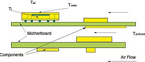
fig. 2: diagram of the temperatures related to equation (1).
the factors that affect each of the terms in equation (1) are now briefly listed:
| tambient |
- system level parameters - machine ambient, altitude |
| dtairheating |
- system level parameters - air-flow rate, air density, humidity board level parameters - component location, power of upstream components, board thermal properties |
| dt case-air |
- system level parameters - air-flow rate - board level parameters - air flow distribution, convection coefficient, board thermal properties - component level parameters - package construction, chip power |
| dt j-case |
- system level parameters - air-flow rate - board level parameters - air flow distribution, convection coefficient, board thermal properties - component level parameters - package construction, chip power |
the factors affecting the tambient and dtairheating are somewhat self explanatory. the last two need a little more explanation and the factors may become clearer to the reader after completely reading the paper, especially with the example of the tbga. for the temperature rise from the case to the air, it is clear that a larger air flow rate will increase the convection coefficient, decreasing this temperature rise. also, the board construction and the package construction determine what percentage of the chip power will be dissipated directly through the case to the air, thus affecting the case-air temperature rise.
for the temperature rise from the case to junction it is easy to see how it is affected by the package construction and chip power. also, the board details affect the percentage of the heat flowing from the junction to the case. the total air flow rate affects the air flow distribution around the boards because the friction factors and flow impedances are a function of the air flow rate. the air flow distribution, for example, at the top of the module vs. back side of the card affects the percentage heat flowing in a direct path from the junction to the case of the module, in turn affecting the junction to case and the case to air temperature rises.
it is beneficial to define the three commonly used performance parameters dependent upon the temperature rises in equation (1):
| rint = (tj - tcase)/chip power = dtj-case/chip power |
(2) |
| rext = (tcase - tair)/chip power = dt case-air/chip power |
(3) |
| rtotal = rint + rext |
(4) |
it is clear that the aim of the thermal designer should be to design for a low rtotal in the system conditions in which the package will be used. the module and system interactions and their impact on rint and rext will now be illustrated with a tbga example.
ibm tape ball grid array (tbga) package study
the ibm tbga offers desirable features such as thin and light construction, flexible custom designs, sizes and lead counts, cte matching to card for excellent reliability, tcb or flip chip interconnect and excellent electrical and thermal performance capability. in this paper, the computational results for a 40 mm body size tbga are used to illustrate the system and component interactions. most of the underlying methodologies and conclusions reached are applicable to other organic packages such as the flip-chip bga.
the schematic diagram of the tbga package is shown in fig. 3. the package size is 40 mm x 40 mm, with 671 solder ball i/os with a 14.6 mm chip. the card size is 76.2 mm x 76.2 mm x 1.6 mm thick (3" x 3" x 0.063") and has 2 or 1 or 0 copper power planes, 0.036mm (1.4 mils) thick. the chip is attached to a kapton (trademark of dupont co.) tape using the c4 (controlled collapse chip connection) technology. the kapton tape consists of a top copper signal layer, the kapton dielectric layer and a bottom copper power plane layer. a copper stiffener with an inside window of 19mm is attached to the tape all around the silicon chip. a copper cover plate is attached to the stiffener and the chip using another adhesive for protection and heat sinking.
the direct heat path is from the chip through the chip attach adhesive into the cover plate and the air. the indirect path is through the c4 bumps - tape - solder balls out through the card to the air on the back. the direct attachment of the cover plate and the dual paths result in superior cooling capability. this, however, complicates the analysis of this package since the card plays a significant role in the thermal management of the package.
this effect is often estimated incorrectly in the determination of the 'package' thermal performance for comparing different packages.
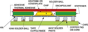
fig. 3: schematic cross section of the tape ball grid array package.
mathematical formulation
due to the complexities in the package and the flow, a detailed, extensive numerical model was developed to predict the heat transfer characteristics of the tbga package. material properties and the thicknesses of the different blocks are given in ref. 4.
the air is assumed to be non-participating in thermal radiation, and both the surfaces of the card as well as the cover plate are assumed to be gray and diffuse. the card surfaces and the tbga cover plate (the module case) are allowed to have radiation exchange with the ambient environment.
several researchers have proposed and used 2nd order schemes such as the (symbol here) model for computing turbulent flow and heat transfer around electronic packages. the widely used standard κ- ε models are valid for fully turbulent flow such that the reynolds number, re > 104, based on hydraulic diameter (ref. 3). such re regimes are rarely encountered in air-cooled electronic packages.
moreover, the κ- ε models involve the solution of two additional coupled equations and are numerically expensive (ref. 3). the results shown here use a simplified approach for the turbulence model, which is shown to work quite well (ref. 4). the c4 and the solderball constriction resistances are accounted for in the model. the emissivity of the card surface and the tbga cover plate were measured by comparing radiation from these surfaces with that from a gray, diffuse surface of known temperature and emissivity.
a detailed grid size study was done to attain a compromise between cost and accuracy. for the turbulence model runs an 81 x 31 x 51 non-uniform grid was used to resolve the sub-layer.
tbga thermal results
experiments were performed to complete a verification of the model by comparing the numerically obtained temperatures with the experimentally measured values. the comparison was intended to verify that all of the simplifications, material properties selected and boundary conditions used in the model were adequate. the experiments were run at the ibm advanced thermal engineering laboratory in endicott, ny. a detailed description of the experimental set up and procedure is given in ref. 5.
figure 4 shows the total thermal resistance as a function of chip power dissipation in the range of 1 to 10 w, in natural convection. the experimental results for two power planes is seen to be in excellent agreement with the numerical predictions. numerical results are compared for a card with no, one and two power planes. the effect of power planes on chip junction temperatures is seen to be very significant. the presence of even a single power plane improves the thermal performance significantly. this clearly shows the effect of the board properties on the total thermal performance.
the junction to air temperature rise per unit power (in other words, rtotal) decreases with an increase in power due to more vigorous convection and higher convective velocities. radiation heat transfer is a significant factor in enhancing the cooling from packages in the natural convection mode and must be included in an analysis (ref. 4).
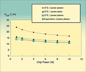
fig. 4: experimental comparison of the experimental and cfd
results for natural convection. also shown is the effect of
the power planes.
table 1 (overleaf) shows the rint and rtotal for the same tbga package for a power of 4 w in natural convection and velocities of 1 and 2 m/s. it is seen that the rint is a very small portion of the rtotal in all the three flow cases because, the temperature drop from the chip to the case is much smaller than that from junction to air. therefore, it is most important for the thermal designer to concentrate on lowering the resistance from the case to the ambient by intelligent flow management to improve cooling in this case. thus, the system air-flow has a profound effect on the rtotal.
also the rint is affected by the flow condition, though to a much smaller extent, as seen in table 1. however, if the extent of flow is changed only on one side of the card, rint may be affected to a much greater extent by such a change in the flow conditions.
table 1
| rint and rtotal for a card with 2 power planes (experimental data), chip power=4w. |
| flow condition |
rint (c/w) |
rtotal (c/w) |
| natural convection |
0.31 |
12.8 |
| 1m/s |
0.30 |
9.0 |
| 2 m/s |
0.33 |
7.5 |
table 2
| rtotal (c/w) cap vs. capless (numerical predictions), chip power = 4 w |
| flow condition |
capped |
no cap (bare die) |
| natural convection |
12.6 |
17.1 |
| 2 m/s |
7.7 |
10.4 |
since the junction to case resistance parameter can change with flow conditions, the thermal designer must evaluate a particular package based on the final application conditions and not merely on comparing the rint of two packages. the total performance in the system must be evaluated.
cfd simulations of the tbga package without the cap or cover plate (ie. with bare die) reveal some more interesting characteristics. since there is no case temperature, ie. the chip itself is the case, the rint value is 0 or very nearly zero. thus the thermal designer, when presented with data for rint for the two packages may be tempted to choose the uncapped module because it has much lower rint. this may be the case even if the comparison is done using a thetaj-c comparison, since thetaj-c measures the resistance from the junction to the case and it will be nearly 0 for the uncapped module and of the mathematical order of 0.1 for the capped module.
however, as the results show in table 2, the junction temperature for the capped module will be lower since the rtotal is much lower. this is due to the fact that with the cap, the area of dissipation from the module top is 40 x 40 = 1600 mm2 as opposed to 14.6x14.6 = 213 mm2 for the bare die; coupled with the fact that in the capped case, a superior adhesive with high low thermal resistance is used for attaching the cap to the chip.
in another illustrative example, consider two packages in an air-cooling test, i.e. the package mounted on a card in air cooling. from experimental data, an overmolded 54 mm bga package under similar airflow conditions and card construction, has an rtotal of approximately 7°c/w compared to the 9°c/w in table 1 for the tbga. looking at these two equivalent data from an aircooling test, the designer may be tempted to choose the one with the lower rtotal ie. the overmolded package. if it so happens that the system has double-sided components, which are very closely spaced on both sides in arrays, the primary heat transfer path is expected to be from the top of the module.
in that case, the tbga is expected to perform better due to the low resistance path from the chip to the top of the module compared to the overmolded bga. thus the designer would have selected a package with a worse performance in the actual system. these examples clearly illustrate that the thermal designer must carefully evaluate the performance of the package in the system in which it will be used. choices based on the package characteristics or standard air-cooling tests alone may not lead to optimal solutions.
summary and conclusions
the effects of the system, board and package parameters on the junction temperatures are explained qualitatively as well as through the examples of bga packages. the paper shows that the thermal designer must consider the performance of a package in the actual system in which it will be used.
solutions based on the resistances or a combination thereof, or even the performance results from a standard air-cooling test alone, may not lead to optimal performance.
sanjeev sathe
ibm microelectronics
1701 north street
endicott, ny
bahgat sammakia
ibm microelectronics
1701 north street
endicott, ny
references
| 1. |
andros, f. e. and sammakia, b.g., (1989), "thermal management in electronic packaging", in principles of electronics packaging, edited by seraphim, d.p., lasky, r. and li c.y., mcgraw hill, new york. |
| 2. |
bar-cohen a. and kraus, a.d., (1988), advances in thermal modeling of electronic components and systems, vol. 1, hemisphere publishing corp. |
| 3. |
gibson, m.m., jones w.p and whitelaw, j.h. (1995), "turbulence models for computational fluid dynamics," thermofluids section report, tf-94-10, imperial college of science, technology and medicine, u.k. |
| 4. |
sathe, s.b. and sammakia b.g. (1996), "a numerical study of the thermal performance of a tape ball grid array (tbga) package", asme heat transfer development, vol. 329, pp. 83-93. |
| 5. |
sathe, s.b., kosteva, s.j., stutzman, r.j. and sammakia, b.g. (1995), "powerpc 60x family of products: thermal management overview", ibm technical report #tr01.c780. |
|


