|
today’s electronics are becoming smaller and faster, resulting in increased power densities and greater risk of thermal problems. thermal dissipation requirements thus need to be satisfied by the use of several cooling mechanisms. the cooling systems may include conduction, convection and radiation cooling. conduction can be the most efficient mode of heat transfer and about 80% of the heat generated in a chip can be dissipated through the printed circuit board.
conventional printed circuit materials are often incapable of guaranteeing sufficient heat dissipation. thermal management is dealt with in a number of ways, including integral thick power/ground planes, bonding of the boards to heat sinks, the use of cut outs which allows the component to be mounted directly on the heat sink, as well as the use of thermal vias or heat slugs designed to carry more heat away from the component. thermal vias and heat slugs are designed to lower the spreading resistance, which can be significant if the footprint of a heat source is much smaller than the footprint of a heat sink that is attached to the circuit board.
the advantages of the conventional printed circuit board approach are their widespread availability, ease of manufacturability, and low cost in volume. unfortunately, the polymer materials typically used to manufacture circuit boards are very poor thermal conductors. increasing the amount of copper in the circuit layers can improve that situation to a degree.
aside from copper, other materials have been used as cores inside a multilayer printed circuit board, including aluminum, various alloy constructions, as well as more sophisticated metal-matrix composites. the latter are also designed to constrain the organic printed circuit boards by providing a low coefficient of thermal expansion (cte). on the other hand, aluminum has often been used as a heat spreader in many surface mount applications because of its low weight, high thermal conductivity and low cost.
thick film ceramic substrate technology offers higher heat dissipation. this is especially true with substrates such as beryllia and aluminum nitride, while the most common ceramic substrate, alumina, does not have very high thermal conductivity. most current under-the-hood automotive applications use hybrid thick film circuits on ceramic substrates. the hybrids are made by additive or parallel processing, but the processing temperature is high (600 -1400°c). the main impediment for their wider use is the very high, often prohibitive, cost.
use of metal circuit boards
electrically insulated metal substrates offer a low cost alternative to ceramic boards. metal substrate circuitry consists of a metal base plate onto which a copper conductor layer is attached with a thermally conductive epoxy dielectric (1). in addition to aluminum, metal substrates such as copper, copper-clad invar and copper-clad molybdenum are suitable as substrates. an aluminum alloy is usually chosen for the base metal for its excellent heat dissipation ability, mechanical integrity, low cost and lightweight construction. other metal substrate constructions laminate 2-layer circuits to a metal substrate, while some board constructions create the 2-layer circuits directly on the anodized aluminum core (2).
comparison between heat dissipation of a cu-clad fr-4 board and a circuit on an aluminum substrate is shown in figure 1. temperature measurements were performed using infrared imaging with emissivity correction (3). with different levels of input power, temperature distributions were obtained for cu-clad fr-4 substrate and for additively processed circuitry on anodized aluminum. thermal resistance of the cu-clad fr-4 board was measured at 5.3°c/w, while that of the circuit on aluminum substrate was measured at 0.8°c/w. this shows the thermal advantage of having the circuitry on metal substrates.
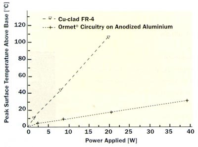
figure 1 – peak temperature measured as a function of power applied for fr-4 and metal substrates.
insulated metal substrates have been in use for thirty years (4), but their popularity has increased recently in applications where mechanical strength and rigidity are desired for single-sided boards. the major problem with most insulated metal board technologies is that they are generally not capable of providing multilayer circuitry.
multilayer circuits on metal boards
a new interconnect circuit technology has been developed. it creates multilayer circuits on metal substrates for excellent thermal dissipation and mechanical stability. multilayer circuits are fabricated directly on one or both sides of a metal base plate by sequential deposition of polymer insulator materials and conductors. the processes utilize in part photoimageable polymer materials to build planar layer-to-layer interconnects (5).
the conductor materials are a combination of a metallurgical composite (ormet) and plated copper. the damascene-like process, in which the conductor is deposited over a patterned insulator material, creates fully planar structures at each layer. this provides the capability of accurately controlling conductor thickness (for added current-carrying capability) and dielectric separation (for controlled impedance applications).
the additive process technology described is used to build circuit boards on metal substrates insulated by only a thin layer of polymer or ceramic. in this type of structure, the board acts as a very efficient, integral heat sink. suitable metals such as aluminum alloys have excellent thermal conductivity and are comparable in cost to standard glass reinforced polymer substrates.
single sided substrates are one application of this multilayer sequential-build-up technology on metal cores. the additive microvia-enabled circuitry does not require through hole connections to create surface-mount boards. there are a significant number of circuit board applications in which it is desirable to leave the entire back surface of the board free of circuitry and components to facilitate the rapid extraction of heat. figure 2 shows the top view of a single-sided metal circuit board.
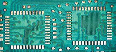
figure 2 – surface mount, metal substrate, multilayer circuit
(with lower levels of circuitry visible).
the resulting circuits are thin and coplanar in profile with the dielectric layer. each circuit and via layer is defined by the thickness of the dielectric layer. multilayer circuits have been demonstrated using this process. 100 μm lines and spaces with 100 μm vias located right on top of and underneath lines of the same size are possible. with the layer-to-layer build-up process, solid via-in-pads and via-in traces are possible.
the additive nature of the technology does not require the large capture pads needed in conventional printed circuit substrates with drilled and plated through holes. this allows blind, buried and stacked vias at any location, all critical factors in developing high-density interconnect and substantial real estate savings. a cross-section schematic of a multilayer structure is depicted in figure 3. it shows the stacked solid vias and circuit traces, as well as the via-in-pad constructions.
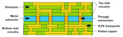
figure 3 – cross-section schematic of a double-sided interconnect metal substrate pcb.
multilayer metal substrate designs were tested for their thermal performance. a 4-layer circuit was fabricated on an aluminum substrate. thermal resistance between the mounted component case and the backside of the board was measured at 3.2°c/w. this value was less than half of the value for a conventional circuit board substrate.
references
1 for example: thermal clad thermal management substrate, bergquist company.
2 p.l. straub, “thermal management for pcbs”, future circuits international, issue 5, pp. 79-82, 1999.
3 j. mcdonald and g. albright, “microthermal imaging in the infrared”, electronic cooling, vol. 3, pp. 26-29, january 1997.
4 d. dinella, “an insulated metal printed wire board”, the western electric engineer, vol. 9, pp. 24-29, july 1965.
5 p. gandhi, “fine-line applications of ormet transient liquid phase sintered conductive ink”, circuit world, pp. 43-46, jan. 1996.
goran matijasevic
ormet corporation
|


