|
by dr. kamal karimanal, customer support engineer
icepak team, fluent inc.
the magic of thin conducting plates
the use of a "zero thickness" planar object for avoiding small cell volumes is no new trick to
users of finite volume-based thermal analysis software. contact resistance plates are often used for modeling temperature jump due to 1-d heat flow across an imperfect contact. similarly, you can use thin conducting plates as zero thickness geometry objects to model interfaces where 3-d conduction cannot be ignored. copper planes in pcb and ic packages are a good example.
the thin conducting plate model in icepak solves the full 3-d conduction equation using finite volume cells that do not extend outside the plane, which eliminates undesirable grid bleeding in the fluid regions.
ic package models - 3 approaches
thermal models of ic packages help to resolve both package design issues and the overall
system design concerns. the level of detail needed varies depending on goal of the analysis. a single thermal model will rarely deliver the goods for both the ic package designer and the overall system designer.
in order to address the wide spectrum of design needs, icepak offers three categories of ic package models. these models are automatically generated by macro programs that use key parameter input from a library of more than 500 jedec standard package outlines.
the three categories are detailed package models, network resistance models, and compact conduction models (ccm).
detailed package models
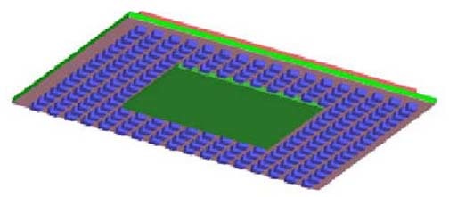
in this approach, all thermally relevant information is captured in the geometry. this includes ball arrays, thermal vias, trace layers, wire bonds, leadframes, and more. figure 1 shows a detailed pbga type package. such a detailed package model may be warranted when the design interest is the package itself.
at this level, the designer is interested in seeing the significant heat flow pathways and determining if the pathways are sufficiently cooling the device. this type of analysis is often useful for selecting the best and most cost efficient package type for a given, application specific board condition.

figure 1. detailed bga model.
network resistance models
on the other extreme is the network resistance model. icepak's advanced unstructured meshing technology allows two star and shunt resistance models to be generated from a single network object (see figure 2).
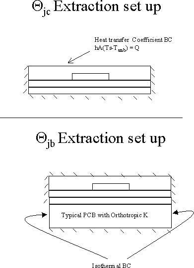
while technology enables elegant implementation of network topologies, the key is knowing the resistance values. in icepak, macros based on standardized network value extraction procedures allow for the creation of automatic extractor models with minimal effort from you. figure 3 shows theta jb and theta jc generation models.
the simplicity of the network resistance objects empowers you to predict junction temperatures of many components in large system level models.

figure 2. icepak's 2 resistor network model.

figure 3. theta jc and jb extraction set up.
compact conduction models (ccm)
this approach represents repetitive and intricate geometry features, such as solder ball arrays, lead arrays, wire bonds, and substrates with copper traces as lumped objects with effective thermal conductivity. other features of the model such as the die, the die pad, and mold compound are modeled as simple solid blocks. figure 4 shows the difference between a detailed and compact model of a pbga.
this modeling approach has advantages, such as:
- the die as well as case temperatures are accurately predicted, as opposed to the two star and shunt network models which are not even meant to predict surface temperatures.
- boundary conditions are independent, since the 3-d heat flow pathway is captured by the model.
- no optimization is necessary, since the models are physics based.
- since actual materials are used to build the package model, it can be used for transient analysis.
while lumping hundreds of balls or leads results in major reduction in mesh sizes, there were some issues that prevented their use in system and sub-system level models, such as:
- die temperature is sensitive to heat spreading in some very thin (~100 mm) features such as the die pad. it is inevitable that such thin features lead to thin elements. the problem is exacerbated in structured cartesian meshes in which the thin elements extend all the way across the domain.
- the varying thickness of the modeled features results in a geometry with several in-package edges that again lead to grid bleeding across the computational domain.
figure 4. cross-section of detailed and compact package models.
thin conducting plates to the rescue
the advent of the thin conducting plate feature in icepak makes ccm a much more appealing option at the system level. if you look at the last graphic in figure 4, it is apparent that thin conducting plates eliminate the need to model the real thickness of the die and the die pad, thus aligning them.
this results in the side view of the package having a single intermediate edge and manageable object thickness. now, there is no reason why ccm can not work at the system level.
validation
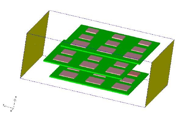
figure 5 shows a 3- board system with 9 packages per board. ccm of 3 different package types, a 128 ball pbga, 208 ball cavity down bga, and 208 ball fpbga were used. the validation procedure involved comparing die and case temperature predictions from an all-ccm model and a reference model.
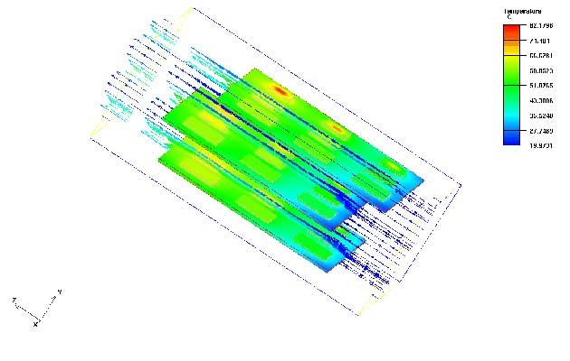
the reference simulation modeled all packages as compact except for one pbga, which was modeled in full detail. figure 6 shows the contour plot from icepak simulation of this model.

figure 5. system with 27 compact bga packages.

figure 6. countour plot from system level model using 27 compact packages.
results
the mesh count for the all-ccm model was 125,000 cells, whereas it was 800,000 for the reference model. the main cause for the high mesh count was the array of 128 balls, which were modeled as equivalent cuboids.
the difference in die, as well as case temperature between the detailed and the simplified models was less than 2%. thus, using ccm resulted in major time savings without any significant compromise in accuracy.
macros & documentation for detailed, simplified and network resistance set up & documentation can be downloaded from: http://www.icepak.com/user/login/parts/pack-macro/index.htm.
|