|
a team of engineers at stanford university have developed a method for producing molybdenum disulfide crystals that are only three atoms thick but large enough to form a chip, in what could be a breakthrough for the mass-production of atomically thin materials for electronics.

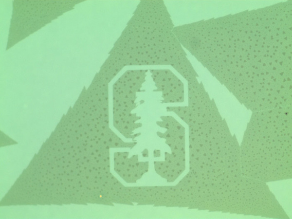
the researchers put the stanford logo on the atomically thin chip. (eric pop/stanford)
the new process, which was documented in a recent article on the stanford website, used chemical vapor deposition. in this process, small amounts of sulfur and molybdenum are burned until the atoms vaporize and then deposited on a substrate (could be glass or silicon).
after placing the monolayer on the substrate, the researchers demonstrated the possibilities of manufacturers could turn the single layer of molybdenum disulfide into a chip by etching the stanford logo and the two candidates from the recent u.s. presidential election onto the prototype.
in the article, electrical engineering associate professor eric pop said of the fun etchings, “we hope ‘nanotrump’ and ‘nanoclinton’ can broaden the interest in research. perhaps seeing portraits etched into a three-atom-thick canvas will inspire future researchers in ways we can’t even imagine yet.”
the research team published its report in 2d materials. the abstract stated:
“we demonstrate monolayer (1l) mos2 grown by chemical vapor deposition (cvd)with transport properties comparable to those of the best exfoliated 1l devices over a wide range of carrier densities (up to∼1013 cm−2 ) and temperatures(80–500 k).
“transfer length measurements decouple the intrinsic material mobility from the contact resistance, at practical carrier densities(>1012 cm−2 ). we demonstrate the highest current density reported to date (∼270 μa μm−1 or 44 ma cm−2 ) at 300 k for an 80 nm long device from cvd-grown 1l mos2.
“using simulations, we discuss what improvements of 1l mos2 are still required to meet technology roadmap requirements for low power and high performance applications. such results are an important step towards large-area electronics based on 1l semiconductors.”
read the full report at http://poplab.stanford.edu/pdfs/smithe-cvdmos2-2dmat16.pdf.
|