|
a team of researchers has released a report stating that the thickness of gallium nitride (gan) layers can impact the thermal budget of a device and, utilizing computer simulations, that the thinner the layer of gan the more heat is dissipated. this only works to a certain point before the layer becomes too thin and the effects are reversed.

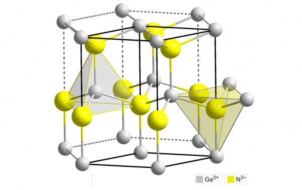
gallium nitride. (wikimedia commons)
according to a report on compoundsemiconductor.net, “the optimal layer size is tied to the device's thermal boundary resistance (tbr), which is a condition that exists at the very interface of gan and other epitaxial layers.”
the abstract of the researchers report stated:
“here, we investigate the effects of thermal boundary resistance (tbr) and temperature-dependent thermal conductivity on the thermal resistance of gan/substrate stacks. a combination of parameters such as substrates {diamond, silicon carbide, silicon, and sapphire}, thermal boundary resistance {10–60 m2k/gw}, heat source lengths {10 nm–20 μm}, and power dissipation levels {1–8 w} are studied by using technology computer-aided design (tcad) software synopsys.
“among diamond, silicon carbide, silicon, and sapphire substrates, the diamond provides the lowest thermal resistance due to its superior thermal conductivity. we report that due to non-zero thermal boundary resistance and localized heating in gan-based high electron mobility transistors, an optimum separation between the heat source and substrate exists.
“for high power (i.e., 8 w) heat dissipation on high thermal conductive substrates (i.e., diamond),the optimum separation between the heat source and substrate becomes submicron thick (i.e., 500 nm), which reduces the hotspot temperature as much as 50°c compared to conventional multi-micron thick case (i.e., 4 μm).
“this is attributed to the thermal conductivity drop in gan near the heat source. improving the tbr between gan and diamond increases temperature reduction by our further approach. overall, we provide thermal management design guidelines for gan-based devices.”
this could be a step forward for the thermal management of high-powered devices, as the researchers determine the optimal layer of gan and its thermal properties. next, the researchers will turn to electrical conductivity.
read an article about the findings at https://www.compoundsemiconductor.net/article/100337-thinner-is-cooler-for-gan-devices.html.
the full report can be found at http://scitation.aip.org/content/aip/journal/apl/109/15/10.1063/1.4964711.
|