|
introduction
semiconductor junctions offer many useful properties including inherent characteristics which are well suited to temperature measurement. within the electronics cooling arena, these properties form the basis for "the electrical method of junction temperature measurement" and are used for measurement of junction temperatures within operating semiconductor devices. they offer the unique capability to measure temperatures deep inside solid state devices, without direct mechanical or optical contact.
methods based on these properties can be applied to virtually all semiconductor device types, spanning the spectrum of semiconductor applications and functionalities. in addition, the limiting measurement bandwidth is high enough to capture all but the fastest thermal device-transients. for these reasons, electrical measurement of semiconductor junction temperatures offers unique advantages over other measurement techniques within this particular context.
temperature-sensitive parameters
there are numerous temperature-dependent electrical phenomena in semiconductor devices that can be harnessed for the task of temperature measurement. these "temperature-sensitive parameters" are commonly known as tsps. there is a wide variety of tsps with varying degrees of desirability. the most ideal characteristics for tsps are described below.
ideal characteristics of a tsp
- sensitive: tsp sensitivity should be "sufficiently high". this sensitivity is expressed in terms of the ratio of voltage change to temperature change and is the tsp temperature-derivative. high sensitivity improves the electrical signal-to-noise ratio and thus the temperature measurement accuracy. insufficient sensitivity yields excessively noisy data.
- non invasive: there should be minimal parasitic electrical heating of the semiconductor associated with the measurement technique. this situation eliminates the need to compensate for self-heating artifacts. ideally, the temperature to be measured is not influenced by the measurement method.
- uniform: there should be sufficient uniformity in the tsp relationship within a production lot of "identical" devices to avoid the need to perform a complete device calibration for every individual device tested.
- linear: the tsp should ideally be a linear or nearly linear function of temperature versus voltage. more non-linear tsps are usually less accurate and more difficult to use.
when considering the use of new or unfamiliar tsps, disappointments and difficulties can be avoided by applying the above criteria.
many tsps are device-type specific. the following table details some commonly used tsps, although this should not be considered an exhaustive list.
| some common tsps |
| diode forward voltage |
diodes, functional ics, bipolar transistors, mosfets, thyristors, thermal test dies |
| saturation voltage |
bipolar transistors, igbts |
| gate turn-on threshold |
mosfets, igbts |
the "numero uno" tsp
the most commonly used tsp is the diode junction voltage generated by a "small", forward biased, constant current flow. it is instructive to compare this tsp to the ideal characteristics listed above. this tsp yields a nearly linear relationship between the voltage and temperature with a typical tsp sensitivity of about 430°c per volt (2.3 mv per °c) for silicon junctions. [1] the equation for computing junction temperature from the measured diode voltage is the familiar straight line equation:
tj = m * vf + t0
where tj is the junction temperature, m is the slope or derivative of the tsp expressed in terms of °c per volt, vf is the diode forward voltage and t0 is the ordinate-intercept or offset temperature. this calibrating equation permits the computation of tj from a measured vf once the calibrating parameters, slope, m, and temperature offset, t0 have been determined.
within a production lot of "identical" devices, the slope (temperature-to-voltage derivative) is nearly constant for most device types. generally, only the offset temperature (intercept) varies among "identical" devices. (figure 1). this variability can be eliminated by adjusting the offset temperature on a device-by-device basis using the known, pretest room temperature as a calibration data point. this procedure is often referred to as "one-point recalibration" and reduces the need for complete device calibrations to only the first device of a specific type tested. (figure 2).
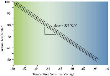
figure 1: temperature versus voltage example for a sample of "identical" devices.
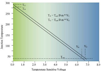
figure 2: illustration of one-point recalibration.
the device calibration for the diode voltage tsp is specific to the chosen "small" forward-biased current, commonly termed the "sense current". based on the second ideal tsp criterion, above, this sense current should not generate significant heating in the junction and thereby artificially elevating the temperature to be measured. although smaller sense currents generate less self heating, smaller sense currents are not always better. two lower limits apply to the selection of sense currents.
- conduction lower limit: the sense current must be sufficiently large to establish conduction in the body of the junction rather than just a superficial leakage conduction. generally 0.1 milliamp is the lower limit of the selection range for the smallest junctions tested. typically, larger junctions have higher lower limits on sense current.
- electrical lower limit: all semiconductor junctions have parallel parasitic electrical capacitances. these capacitances cause the measured diode voltage to lag the true semiconductor temperature-dependent voltage. this lag condition generates problems for functional device testing. such electrical transient durations can range as high as 500 microseconds and are reduced by larger sense currents. again, the larger the junction, the larger the appropriate sense current.
generally, 1 milliamp sense currents are used for all except power semiconductor devices where sense currents of 10 or 20 milliamps are common. a silicon junction passing 1 milliamp typically drops about 0.6 volts and therefore dissipates about 0.0006 watts as an integral part of the temperature measurement. a typical ceiling for junction-to-ambient thermal resistances is about 500 °c per watt yielding an insignificant upper limit in the artifact of 0.3 degree at 1 milliamp. given this, 1 milliamp is the most justifiable and widely used sense current for low power devices. for power semiconductors, 10 milliamps is common although with an even smaller artifact ceiling. actually estimating the artifact for any given test situation is beneficial for sense current selection.
clearly, the properties of the diode voltage tsp compare quite favorably with ideal tsp characteristics listed above. this fact to great extent accounts for the popularity of the diode voltage tsp.
device calibration
once a tsp has been chosen, the relationship between the electrical entity (usually voltage) and temperature must be determined through a process known as "device calibration". device calibration involves forcing the semiconductor to a known temperature and then measuring the tsp voltage associated with that temperature. this procedure typically involves an isothermal dielectric bath, although an oven with a heat sink can be used. after performing this procedure over a span of temperatures, an equation relating temperature and voltage can be derived to express this data.
thus the "calibrating equation" expresses the tsp and essentially renders the calibrated device a temperature sensor. the most accurate method of device calibration implements numerous calibration temperatures, chosen to evenly span the range of semiconductor operating temperatures.
one vitally important aspect of device calibration is the determination of accuracy and the typical error bounds for the temperature measurement. these errors stem from three sources:
- random errors associated with tsp measurement: these random errors are those associated with making the electrical measurement. proper shielding and grounding, instrument calibration, and an adequately sensitive tsp will reduce these errors.
- systematic errors in device calibration procedures: device calibration data is comprised of the tsp voltage and the corresponding temperature of the semiconductor. this semiconductor temperature is typically measured with an external contact sensor on the outside surface of a packaged semiconductor device (figure 3). depending on the time-temperature history of the device, the outside surface temperature may not be equal to the internal temperature of the semiconductor. this situation introduces a systematic error into the device calibration data.
- accuracy of data representation: these errors are associated with the formulation of the calibrating equation as a representation of the tsp data. a calibration based on two data points will not reveal a non-linear tsp characteristic, or provide the accuracy enhancement of data averaging over a range of temperature data.
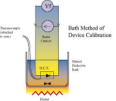
figure 3: calibration bath.
during device calibration, data should only be taken once thermal equilibrium has been reached by the device within the calibrating environment. since the device under calibration is only heated by the minute self heating artifact generated by the sense current, the outside surface of the device will nearly equal the internal temperature of the semiconductor once equilibrium with the environment has been reached. prior to this condition, the calibration environment (bath liquid) must remain steady for a sufficient period of time.
the waiting time then for equilibration from the outside to the inside of the device is determined by the heat capacity of the device and the thermal resistance between the device junction and the calibrating medium. a stirred liquid bath provides an excellent calibration medium to minimize this waiting interval. generally, the larger the component under calibration, the longer the waiting interval. these considerations are essential to controlling systematic device calibration errors.
device characterization
measurements of thermal impedances and resistances associated with packaged semiconductor devices can be performed by measuring the junction temperature response to a measured heat dissipation from within the semiconductor. this procedure is termed "device characterization". the electrical method of junction temperature measurement can be used to measure transient and steady state thermal behavior. although the utility of steady state thermal measurements is well established for predicting junction temperatures, the substantial value of transient thermal measurements is commonly overlooked. transient thermal measurements can uniquely differentiate the internal thermal performance of complex thermal packages. [2] this insight is essential to determining the best approach for package enhancement and improvement.
figure 4 illustrates the application of the diode voltage tsp to characterization of a rectifier diode. nearly all functional devices utilize a scheme similar to this where the heating power is alternately switched with the temperature sensing current. the device cannot be both heated and temperature-sensed simultaneously since a heating current and sense current cannot exist at the same time in one device. to overcome this, an electronic switch with extremely brief transitions operates between these two functions and can effectively capture the junction temperature before significant die cooling has occurred. for more information on testing functional devices, see references [3,4].
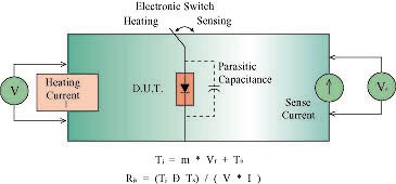
figure 4: diode test setup.
figure 5 illustrates the thermal die test method. thermal test dice are specifically designed for thermal characterization of integrated circuit packages. they are available in a variety of sizes and are popular for package characterizations since both heating and temperature sensing can be performed simultaneously without the need for rapid switching. care must be taken to ensure that the thermal test die size and die attachment matches that of the intended functional die application. due to this matching problem, active or functional dice are often used as the ultimate test vehicle for component thermal characterization.
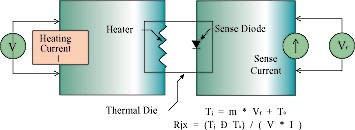
figure 5: thermal test die setup.
conclusions
the use of the electrical method for junction temperature sensing has some of the critical details of implementation that ultimately determine the accuracy and overall success of the method. once some understanding and experience has been gained, it offers a powerful and accurate tool for thermal characterization of semiconductor components.
dr. john w sofia
analysis tech
wakefield, ma
references:
1. integrated circuit thermal measurement method - electrical test method (single semiconductor device), eia/jedec standard, eia/jesd51-1, arlington, va, p. 5.
2. sofia, j.w., "analysis of thermal transient data with synthesized dynamic models for semiconductor devices", ieee transactions on components, packaging, and manufacturing technology part a (cpmt), volume 18, march 1995, pp 39-47.
3. "circuit-performance and thermal resistance measurements" (3100 series) mil-std-750c, february, 1993.
4. oettinger, f.f., blackburn, d.l. "thermal resistance measurements", nist special publication 400-86 from series on semiconductor measurement technology, july, 1990.
|


