|
introduction
infrared imaging methods provide unequaled ease and flexibility for investigating micro-circuit temperatures. the researcher need only slide the circuit under the objective lens and power it up in order to measure the temperatures throughout the micro-circuit at once, precisely and without physical contact. with the infrared instruments available today, workers can measure temperature differences as fine as 20 to 40 millikelvin (equal to milli-degrees celsius) and see spatial features as fine as a few microns.
infrared measurements are not only accurate but also the fastest available and offer the least disturbance to the point being measured. in terms of human bandwidth, the amount of information conveyed is astounding. the researcher literally gets the entire picture of how the heat is distributed over the part and how it is changing in real time. infrared imaging has a decided advantage for navigating under the microscope, compared to methods which require the worker to paint an obscuring liquid crystal or fluorescent material onto the circuit.
micro-circuits present special problems for infrared temperature measurement. they use liberal amounts of metal which makes them very reflective. this reduces their infrared emissions and contaminates their signature with stray emissions reflected from elsewhere in the environment. however, through consistent effort and clever application of the laws of radiation physics, these problems have largely been solved. practical thermal imaging microscopes are now available with point and click operation. in this article, we discuss the fundamentals of infrared physics as they apply to measuring micro-circuit temperatures and we present example images from a typical measurement.
planck's law
every object whose temperature is not absolute zero emits thermal radiation. a fireplace poker or a light bulb filament may not be hot enough to visibly glow, but most of the energy emitted by objects within 50 degrees c of room temperature is emitted within the 3 to 14 µm wavelength region. the fundamental description of thermal radiation is the planck blackbody radiation law:

| where |
|
| q |
is in photons per second per cubic centimeter and gives the thermal photons distributed over wavelength, emitted into a hemisphere from a given source area |
| c |
is the velocity of light, 3 x 1010 cm/s |
| h |
is planck's constant, 6.63 x 10⁻³⁴ watts/s2 |
| k |
boltzmann's constant, 1.38 x 10⁻²³ watts s / °kelvin |
 |
is the wavelength in centimeters |
| t |
is the source temperature in degrees kelvin. |
infrared microscopy makes use of this radiation by using detector arrays, such as indium antimonide and mercury cadmium telluride, which are sensitive to infrared wavelengths. these detector materials are available in the form of charged coupled device (ccd) arrays which are two dimensional arrays, much like those used in video cameras. an infrared microscope is constructed by assembling such an array with appropriate infrared optics. a personal computer is added to calculate the device temperature based on the flux received by the detector.
the detector material is usually cooled to liquid nitrogen temperatures. ordinary glass lenses are opaque in the mid to longwave infrared, so infrared microscopes as well as military thermal imagers use exotic lens materials such as silicon, zinc selenide, or germanium. indeed, the number of practical ir lens materials is limited to just 6 or 8 which are not terribly expensive, toxic or soluble in water. this compares poorly with the hundreds of optical glasses available for visible wavelengths, which offer the infrared designer some advantages, such as higher indices of refraction, and it is not too difficult to obtain infrared optics.
the concept of emissivity
planck's law was derived for a "blackbody" - a source which by geometry or material is perfectly efficient in absorbing radiation and is hence "black". the blackbody does not reflect light so any radiation emanating from such a source is derived solely from the thermal properties of that source. unfortunately, microcircuits are made of materials which make notoriously poor infrared sources. to apply planck's law for temperature measurement, we must introduce the concept of emissivity. the emissivity ε of a source is the ratio of its actual radiant emittance to that of a perfect blackbody at the same temperature.

sources which are not perfect are known as gray-bodies or selective emitters. a gray-body is one which emits radiation in exactly the same spectral distribution as a blackbody at the same temperature, but with reduced intensity. a selective emitter is one in which emissivity ε(λ) varies with wavelength.
silicon is a selective emitter but, fortunately, over a small spectral bandwidth, it behaves like a gray-body, permitting us to use classic planck mathematics to infer its temperature, if we know its emissivity. figure 1 shows a map of the emissivity of a typical micro-circuit. the metal layers are clearly visible and the color scale shows that the metal layers have about half the emissivity of the doped silicon.
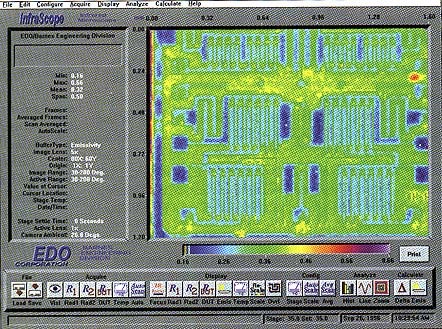
figure 1 - emissivity map for a typical micro-circuit.
what to do about reflected light?
when radiant energy is incident on a surface, three things can happen: a fraction of the energy a may be absorbed; a fraction r may be reflected; and a fraction τ may be transmitted through the part. since energy is conserved the sum of these fractions must equal 1:
α+ r + τ = 1 (eq. 3)
good absorbers are good emitters and empirically it turns out that a material's absorbivity equals its emissivity.
α = ε
using this, we can restate kirchoff's law as:
ε + r + τ = 1 (eq. 4)
any part which is a poor absorber or emitter will be a good reflector or a good transmitter. when examining a part with an infrared microscope, some of the detected radiation inevitably comes from elsewhere, either passing through the part or being reflected from it. this is certainly true of integrated circuits. they are fabricated chiefly from silicon and metal which have particularly low emissivity.
compensating for low emissivities
when emissivities are very low, the instrument is as likely to measure the temperature of the room as it is the part being tested. what the instrument actually measures is three blackbody functions, one for each of the emitted, reflected and transmitted component as in equation 5.

where φ is the integrated photon flux seen by the detector. the emitted radiation is characteristic of ts, the source temperature, and the reflected and transmitted components are likely to be characteristic of the ambient surround at temperature ta. a typical value for ε may be 10% for a metal layer on a micro-circuit, so that if the part temperature and ambient temperature are close, the instrument will detect mostly radiation from the room. fortunately, the flux increases approximately to the 3rd power of temperature so the researcher can make the first term dominate by raising the temperature of the part to be measured substantially above the room ambient.
one method of accomplishing this is to mount the part on a thermoelectric stage and to elevate the base temperature to 70°c or more. this will effectively mask any contribution from the ambient.
pixel by pixel emissivity correction
most infrared radiometers allow no more than a single user estimate for the target emissivity and they employ this single input for all pixels in the image. microcircuits have naturally low emissivity and often 2 to 1 variation in emissivity between metal layers and silicon so this could lead to serious errors. it is therefore more accurate to measure emissivity at each pixel location. since the device is mounted on an opaque substage, we can assume that the optical transmission of light through the device is zero.
equation 1, when integrated over the detector's sensitive wavelengths, can be rewritten as:
nm1=εn1 + (1ε)na (eq. 6)
and again for the source at a different temperature
nm2=εn2 + (1-ε)na (eq. 7)
| where: |
|
| nm1 |
is the radiance measured by the detector with the source at a known temperature. |
| εn1 |
is the radiance corresponding to source at a known temperature and at emissivity ε (as yet unknown) and |
| (1-ε)na |
is the contribution from the room ambient. |
| n |
in these cases is the photon flux integrated over the sensitive wavelengths of the detector n = σq(t,λ)dλ |
by subtracting the two equations the ambient term drops out and solving for ε:

the emissivity for each pixel is the difference between the measured radiance for each temperature divided by the difference between the calculated radiance at each temperature for a perfect blackbody.
by fixing the part firmly to a thermo-electrically driven substage and measuring the radiance of the unpowered device at 2 temperatures, we can calculate the emissivity of the circuit to a high accuracy for each pixel.
limitations
all microscopes have a resolution limit proportional to the wavelength and infrared microscopes utilize long wavelengths. infrared inspection will never offer a resolution approaching the submicron feature size of the latest circuits. the limit of resolution for a microscope is given by the sparrow criteria, which is more aggressive than the better known rayleigh criteria.
where:

d is the minimum separation between features to be resolved
λ is the wavelength of light
n.a. is the numerical aperture of the microscope objective.
without oil immersion, the numerical aperture is theoretically limited to 1, and practically limited to 0.95. in the semiconductor industry, long working distances between the objective and the integrated circuit further limits the n.a. it is convenient to assume an n.a. of 0.5 for which the sparrow criteria is the same as the wavelength. the sparrow criteria is an actual physical limit, which is independent of magnification. additional magnification makes the blurred area appear larger, not less blurred. the current generation of infrared microscopes operates at about 5 µm wavelength, which limits the feature resolution to about the same dimension. research is under way to develop instruments which operate at 2 to 3 µm, but they are not yet available.
an application of planck's law for wavelengths shorter than 1 µm, suggests that there is too little thermal energy at short wavelengths to make such a system practical. current state-of-the-art microthermal imaging microscopes operate between 1.5 to 5.5 microns wavelength with a resolution of about 5 microns and a sensitivity of about 100 milli-kelvin. within those limits there is a lot of information available in a microthermal image, as can be seen in the following examples.
examples
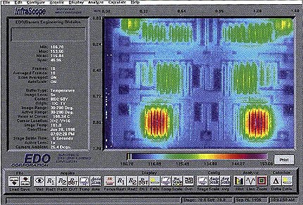
the following example images and the earlier emissivity image were acquired using the edo barnes' infrascope which is capable of resolving 5 micron features and has a sensitivity of about 0.1°c. figure 2 shows a sequence of 4 images. the two radiance images were taken at different substage temperatures and used to calculate the emissivity image, also shown. the fourth image was taken with the part powered up and it employs both the emissivity correction and a correction to remove the background ambient. the temperature image is reproduced in figure 3. the instrument captured 5 separate images to produce this result, all automated and the result of a single mouse click. it took approximately 10 minutes to mount the previously delidded part, and 5 minutes to set up and capture the images.
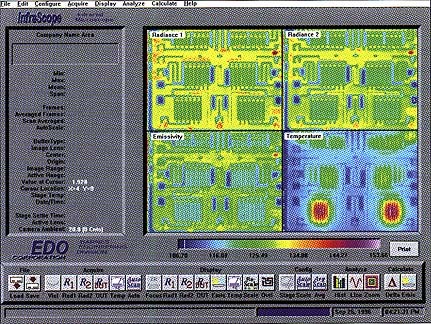
figure 2 - suite of images from microthermal imaging system showing a sequence of two radiance images to find emissivity, followed by power-on-the-ic temperature range.
acknowledgments
thanks to edo barnes engineering division, shelton ct, for the use of their infrascope to make these images.
john mcdonald
latigo optics
malibu, ca
grant albright
edo/barnes engineering division
shelton, ct
references
1. levine, m.a., solid state cooling with thermoelectrics, electronic packaging & production, nov. 1989.
2. melcor corporation, thermoelectric handbook, sept., 1995.
3. rowe, d. m., crc handbook of thermoelectrics, crc press, inc., 1995.
4. smythe, robert, thermoelectric coolers take the heat out of today s hot chips, electronic products, aug. 1995.
for additional information
1. richard d. hudson, jr., infrared system engineering, wiley, 1969, isbn 471418501.
2. warren j. smith, modern optical engineering, mcgraw-hill,1990 isbn 0-07-059174
|