|
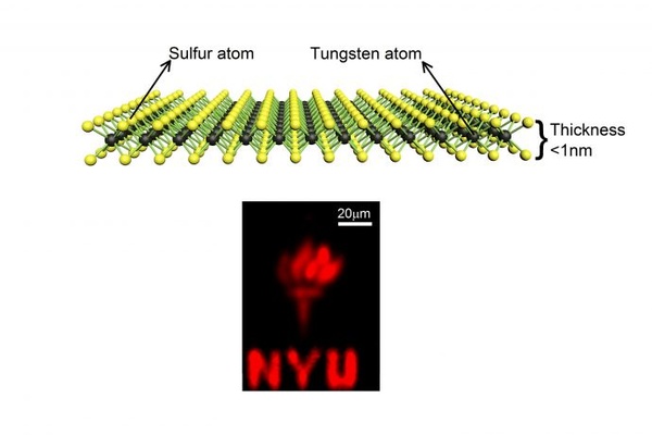
researchers at the new york university tandon school of engineering have developed a method for synthesizing large sheets of monolayer tungsten disulfide, which is a material with a wide range of electronic and optoelectronic applications, according to a report on the nyu website.

the nyu logo showed the energy being emitted from the monolayers. (new york university)
the search for electronic materials at the two-dimensional level has been a quest for scientists, heightened by the discovery of graphene more than a decade ago. these monolayer materials are one-atom thick and have properties such as flexibility, strength, and conductivity that researchers believe will benefit the electronics industry.
at nyu, the engineers grew tungsten disulfide through chemical vapor deposition in a newly developed reactor that produced the highest quality monolayer of the material on record. according to professor davood shahrjerdi, “it’s a critical step toward enabling the kind of research necessary for developing next-generation transistors, wearable electronics, and even flexible biomedical devices.”
an advantage for tungsten disulfide over graphene is that it boasts a wide energy band gap and as the number of atomic layers increased the band gap became tunable. in addition, the monolayer had strong light absorption and emission properties.
the report noted that the engineers had “succeeded in reducing the structural disorders by omitting the growth promoters and using nitrogen as a carrier gas rather than a more common choice, argon.”
the research was published this month in applied physics letters. the abstract read:
“we demonstrate chemical vapor deposition of large monolayer tungsten disulfide (ws2) (>200 μm). photoluminescence and raman spectroscopy provide insight into the structural and strain heterogeneity of the flakes. we observe exciton quenching at grain boundaries that originate from the nucleation site at the center of the ws2 flakes.
“temperature variable transport measurements of top-gated ws2 transistorsshow an apparent metal-to-insulator transition. variable range and thermally activated hopping mechanisms can explain the carrier transport in the insulating phase at low and intermediate temperatures.
“the devices exhibit room-temperature field-effect electron mobility as high as 48 cm2/v.s. the mobility increases with decreasing temperature and begins to saturate at below 100 °k, possibly due to coulomb scattering or defects.”
read the full report at http://scitation.aip.org/content/aip/journal/apl/109/19/10.1063/1.4967188.
|