|
authors:
alex pike, steve jacobs, and mike sickmiller
elo technologies, inc.
abstract
designing for adequate power dissipation in microelectronics systems has become extremely challenging. in some applications, the device integration density is limited by thermal conditions not by lithography, or processing. one example is power amplifiers used in high-frequency communications systems.
power amplifiers present a tremendous challenge to heat sinking which is growing as power density and transmitted power increase in the ever expanding world of wireless communications applications. many of these designs use gallium arsenide for the substrate, which complicates the problem since gaas is such a poor thermal conductor.
elo technologies is developing a unique packaging technology that will significantly improve the thermal performance of gaas-based systems without impacting the electrical operation of the circuit. ultra-thin semiconductor processing techniques are used to thin the substrate to less than 5 mm, in conjunction with backside processing to locate thermal shunts, creating a low-thermal impedance path.
this paper presents thermal simulation results that show how the elo packaging process improves the power dissipation of a gaas-based device. a finite element analysis was performed on a conventional gaas package and on the proposed elo package. simulation results show that the elo package configuration reduces the junction temperature of the device, which improves the operating efficiency, enhances the device longevity, and can lead in increased integration density.
there are several characteristics of gaas-based heterojunction bipolar transistors that make them very favorable for high frequency applications, such as the transmitter stage in a wireless communications system. these devices typically have excellent linearity, high power-added efficiencies, and high power densities. unfortunately, the poor thermal conductivity of gaas combined with the high power density of hbts creates some difficult challenges with respect to thermal management. a primary concern in such systems is to minimize the junction temperature of these devices.
several solutions have been proposed to address the problem; bath-tub thermal shunts [1], flip-chip bonding, air bridges with thermal shunts [2]. elo technologies has developed a new approach using ultra-thin film semiconductor process techniques which allow us to create, manipulate, and package extremely thin (less than 5mm) semiconductor films and devices. using these methods, we can create a gaas-based hbt that exhibits superior thermal performance.
this paper overviews our fabrication process and then present computer simulations on the thermal performance of an elo hbt. we will compare the simulation results of the elo device with the results of a conventionally packaged gaas-based hbt.
elo packaging process
fabrication of ultra-thin gaas-based hbt can begin with an off-the-shelf device. the primary requirement for the elo fabrication process is that an etch-stop layer be located below all the device layers. the process starts with a device definition etch, which extends below the etch-stop layer. this etch will later separate individual die from each other, eliminating the need to perform wafer sawing.
next, a photodefinable polymer is deposited onto the devices. standard photolithography is used to define protective caps on top of each device. this cap serves as a physical handle for each device and as a protective layer during subsequent processing.
an intermediate carrier disk is prepared by spin coating with a proprietary polymer. this carrier disk is next placed into contact with the protective caps on the device wafer. the polymer is cured, firmly attaching the devices to the intermediate carrier. the devices are now ready for substrate removal processing.
substrate removal can be performed with either a chemical or plasma etch. the only requirement is for selectivity to the etch stop layer. following substrate removal, the devices are prepared for backside processing.
one important consideration in creation of these low-thermal resistance devices is electrical parasitics. the high frequency operation of the devices requires the circuit parasitics be kept to a minimum. the method presented here uses backside processing and photolithography to carefully locate thermal vias only under hot spots, the hbt devices. the backside is selectively metallized only under the hbts, which minimizes the electrical impact of the thermal vias. all other areas are filled by a non-electrically conductive polymer.
the final host substrate is prepared by creating solder bond pads. we currently use electroplating to deposit very thin solder bond pads onto a heat sink material. a flip-chip bonder is used to align the intermediate carrier, with the attached ultra-thin gaas devices, to the final substrate. the solder bond is performed under a forming gas environment.
finally, the intermediate carrier is removed by selectively dissolving the coated polymer. we employ a proprietary solvent that removes only the attach polymer. this step completes the elo packaging process. the devices are now ready for wire bonding and final packaging. a diagram of the final elo packaged hbt is shown in figure 1.

figure 1. a diagram of the elo packaged hbt devices.
thermal simulations
the computer program used in the computer simulation work is called thermal analysis software (tas), from harvard thermal, inc. tas uses a finite element, finite difference solution engine to solve the thermal model. using some basic drawing tools, a model is entered into the program as a collection of nodes, plates, and bricks. the node density is very important in developing an accurate model, since temperatures are calculated only at the node locations. in regions of high thermal gradients a greater node density should be used to capture the correct temperature distribution. in the elo model, we anticipated that high thermal gradients would occur in two areas. one region was near the hbt device itself. and the other was in the metal via that extends from the back of the gaas thin film to the heat sink.
high thermal gradients could be expected around the device itself for two reasons. first, the device is the heat source and thus is the hottest part of the model. second, the low thermal conductivity of gaas will act as a barrier to heat flow. the metal via will show a fairly high thermal gradient because it provides a thermal path between two regions at very different temperatures, the gaas thin film and the heat sink.
the next area we examined was that of the power density of the hbt device in the amplifier itself.it is very important to gain an understanding of how much power passes through a given area, as this determines the heat load of the model. several different power amplifiers were examined from published papers showing a fairly wide range of results[3][4][5]. however, most of the amplifiers which operated in class a mode showed a power density of ~7x10⁴ w/cm2.
interestingly enough, both gaas hbts and mesfets were found that exhibited power densities in this neighborhood. using the elo packaging process, much higher power densities should be possible since the design is more efficient at dissipating heat.
the next requirement was to determine what power levels are typically used in wireless communications systems. there are several different cellular telephone transmission protocols currently in place, each has a different requirement on the maximum transmission power. we carefully studied three different systems currently in use in the united states; north america tdma, gsm, and cdma. both the gsm, and na-tdma protocols employ a time division technique where the broadcast time period is divided into slots.
the transmitter is allowed to send only during a fraction of the total slots. in the gsm system, the maximum transmission power for a portable handset is 2 w. however, the average radiated power is 1/8 of that amount due to the time division, or 250 mw. for the na-tdma system, the maximum power is 4 w but is reduced to 1.3 w when averaged over the entire time frame. cdma employs a more sophisticated transmission protocol which allows the transmitter to remain on during the entire broadcast sequence (there are no time slots). thus, under cdma standards, the transmitter is always on. the maximum radiated power by a cdma portable handset is 6.3w

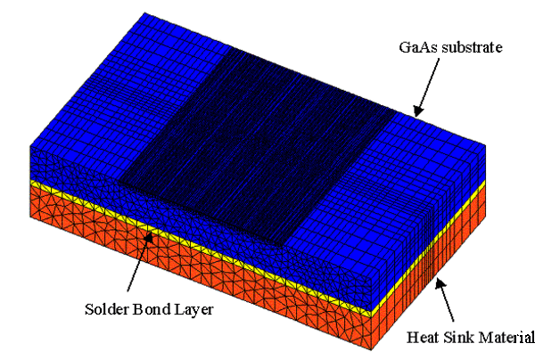
figure 2. a solid fill model of the conventionally package hbt.
the conventionally packaged device was modeled using a commercially available device as a reference. this commercial device was packaged in a conventional manner, using solder die attach to a copper lead frame. the device itself was a gaas-based hbt power amplifier for the gsm 1800 communications network. the die measured 1.6mm x 1.3mm, with a thickness of 125 mm. the die attach solder was modeled as 40mm of sn/pb (63/37).
the device was constructed from 80 emitter fingers with dimensions of 2mm x 20mm, and intervals of 5 mm. the published performance of amplifier was 32dbm with a power added efficiency of 42% [5]. this translates to a dissipated power of 3.77watts. the calculated power density was 6 x 10⁴w/cm2, a typical figure of this kind of system. a solid fill model of the conventionally packaged hbt is shown in figure 2 above.
the elo packaged model employed the same physical dimensions on the chip as the conventionally packaged device, with one very important exception. the gaas substrate thickness was modeled as 5 mm. the die attach materials and dimensions were also altered. in the elo package, a sn/pb (63/37) solder bond is used in the region directly under the hbt devices. an epoxy underfill is used to support and attach the remainder of the die to the substrate. all other structures (emitter finger dimensions, layout, power densities) were kept the same between the two models.
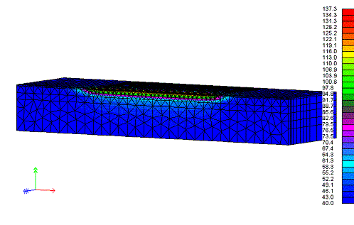
the thermal simulation results revealed some interesting features of the two different packaging implementations. the junction temperature of the hbt devices was substantially lower in the elo package than in the conventional device. with a steady-state power level of 3.8 watts, the conventionally packaged hbts sustained a junction temperature of 227°c, while the elo packaged device reached only 138°c, a difference of nearly 90°c.

figure 4. computer simulation results on the temperature distribution
in a conventionally packaged hbt.

figure 5. computer simulation results on the temperature distribution
in an elo packaged hbt.
the thermal resistance of each package design was found by solving the model for several different power levels. the simulation results showed that the elo packaged device had a 2x lower thermal resistance as compared to the conventionally packaged device (25°c/watt vs. 50°c/watt).
conclusion
we have presented a new approach to addressing the high power dissipation requirements of a gaas-based hbt. using computer simulations, the elo packaged devices showed a 2x reduction in thermal resistance as compared to a conventionally packaged hbt device. several important benefits can be realized from such a drastic reduction in the junction temperature of the devices.
these include longer operating lifetime, improved efficiency, and the potential to increase the circuit density. elo technologies is currently working on fabricating a test device that will be used to verify the simulation results.
references
[1] c.a. bozada, et al microwave power heterojunction bipolar transistors fabricated with thermal shunt and bathtub gaas ic symposium, 1995, p155-158
[2] f. dhondt, j. barrette, p.a rolland 3d finite-difference electrothermal model for multifinger hbts with thermal shunt and emitter ballast resistance, solid-state electronics, vol.42, no. 9, pp.1723-1729
[3] k. yamamoto, et al a 3.2-v operation single-chip algaas/gaas hbt mmic power amperlifier for gsm900/1800 dual-band applications, ieee mtt-s digest, 1999, pp1397-1400
[4] j. griffiths, v. sadhir, a low cost 3.6v single supply gaas power amplifier id for the 1.9ghz dect system, ieee microwave systems conference, 1995, pp37-40
[5] sung-jae maeng, et al a gaas power amplifier for 3.3v cdma/amps dual-mode cellular phones, ieee transactions on microwave theory and techniques, vol. 43, no. 12, december 1995, pp2839-2844
[6] david j. goodman, wireless personal communications systems, addion-wesley, 1997
|