|
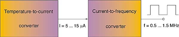
fig.1. block diagram of the frequency output sensor.
introduction
this paper will discuss a new approach to the measurement of the thermal properties of pcbs and the packages mounted to them. it is intended to replace traditional solutions, such as using thermocouples and data acquisition equipment. the basic idea of this approach is that the ic chips themselves will be used to measure and acquire temperature data.
it will be demonstrated that only minimal additional circuitry is required in the ics to achieve this goal. besides the thermal testing, this additional circuitry is suitable for the on-line thermal monitoring of electronic equipment. the temperature sensor built-into the chip ensures that the temperature of the hottest regions is surveyed and the response time between the overheating and sensing is short. experimental results demonstrate the viability of these methods.
conception of a built-in thermal testing system
in the framework of the ec project therminic[1] our research group has dealt for several years with the problems of modifying and completing the chip designs in order to provide a better thermal handling, monitoring and measurability. as an analogy of the design for testability (dft) principle, in a previous paper we proposed that the dftt = design for thermal testability be applied as part of the general design methodology. our approach is: to build into the chips some excess circuitry (as little as possible) in order to facilitate both the production testing and the lifetime thermal monitoring.
based on the previous research and experimental work two different dftt methods appear to be feasible:
method 1: a built-in temperature sensor accompanied with its readout circuitry called henceforth bits.
method 2: the bits circuit together with a controllable dissipator constituting a complete built-in thermal tester (bitt).
the natural way to access both circuits is to use the other test circuitry that is present already in the chip. during our experimental work we used the boundary-scan (bs) architecture because it is a standardized and widely known solution.
the key problem central to any thermal testing/monitoring approach is the temperature sensor that is built into the chip. a suitable solution for this sensor will be discussed.
a suitable temperature sensor
numerous solutions for cmos compatible temperature sensors for thermal testing purposes have been developed by various groups in the past years.
a promising solution has also been developed at tu budapest, as a cmos temperature sensor cell. this circuit is ideal for thermal monitoring purposes and for performing the sensing function in built-in thermal test circuitry.
the sensor circuit consists of 31 small-size mos transistors. the block diagram of this sensor is shown in fig.1. the left-hand side of the circuit is a current-output sensor. the output current decreases as the temperature increases. this operation is based both on the temperature dependence of the threshold voltage and the carrier mobility. the right hand side of the circuit is a current-to-frequency converter, providing a square wave as output signal, the frequency of which is directly related to the temperature.
the experimental realization of this frequency-output temperature sensor, shows strong temperature dependence of the frequency, which can be approximated as;
f = f20cels·exp( ϒ(tcels -20° c))
in the -50.+120°c temperature range, where ϒis the sensitivity, f20cels is the nominal frequency related to t=20°c.
the sensitivity is about ϒ = -0.78%/°c. the output frequency of 0.5-1.5 mhz is in the convenient range. the complete circuit requires only an area of 0.018 mm2 using the ecpd10 [2] 1µm cmos process. using the ams 0.8μm process [3] the area consumption is 0.005 mm2.
the frequency output solution holds an explicit advantage, namely that, the output signal can be processed using purely digital circuitry: for example, counters etc. this means that these sensors can be easily implemented into digital circuits.
the low sensitivity of the supply voltage is a remarkable feature: ±0.25 v change in vdd results and only a ±0.28% change in the frequency. the latter corresponds to a ±0.35°c error. the long-term stability has been investigated in a five-month-long experiment. drift in a definite direction cannot be observed. the total power consumption of the sensor is about 200 µw.
read-out through the boundary-scan path
if a temperature sensor, like the one described earlier is inserted into a chip design, additional circuitry must be implemented in order to provide access to this sensor. additional package pins will also be required.
the excess area consumption and especially the need for additional pins is considered by the ic manufacturers as such an important disadvantage that makes questionable the practical use of the bits solution. fortunately, the built-in temperature sensors can be combined with other built-in test circuitry, effectively reducing the cost.
the boundary scan (bs) architecture is especially suitable for monitoring temperature sensors. in this way it is possible to realize the bits principle so reducing excess circuitry and the need for excess pins.
the boundary scan architecture was developed as a new approach to pcb testing. this architecture has led to a world standard: ieee std 1149.1. if the standard bs circuitry is built into all the ics of a pc board, nail-bed testers can be dispensed with. the wires of the pcb can be observed/controlled in an electronic way, through the bs path. opens and shorts in the pcb wiring, faulty soldering etc., can be easily detected and localized.
the bs architecture can be adapted to implement additional tests: e.g. the testing of the chip core, launching built-in self-test runs, etc.
the bs circuitry is controlled by a state-machine with 16 states called test access port controllers. four pins are allocated to the bs: tdi and tdo for the instruction and data flow organized as a serial scan path, tck is the test clock and tms is the test mode select signal.
the bs architecture is ideal for incorporating frequency-output temperature sensors. an internal counter of 12-14 bits is required in addition to the usual bs circuitry. two excess bs instructions must be defined to enable/disable the sensor and to scan-out the temperature data. the block diagram of a realized extension of a bs circuit is shown in fig. 2. the complete area overhead (shaded blocks) was less than 0.2 mm2 for a 1 µm process.
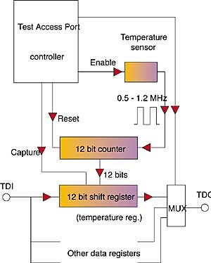
fig. 2. excess blocks required by the bits in the bs circuitry (colored rectangles).
examples of the benefits of the proposed method
a very important use of the bits is the thermal monitoring when (concurrently with the system operation) the chip temperatures are regularly measured. this way the thermal state of a pcb or the entire system can be continuously tested. dangerous overheating caused by the failure of a fan or an over-dissipation in the electronic circuits can be identified in time. preventive actions can then be taken, such as reducing the clock frequency, switching-on reserve fans etc.
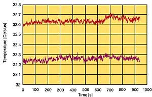
fig. 3. temperature profiles recorded via the bs path
(temperature of two packages on the same board).
temperature measurement through the bs path are presented in fig.3. the pc board was placed in still air. using only the boundary-scan path the chip temperatures were measured every second. a sequence of 940s duration was plotted. a slow random variation of the temperature inside the chassis is evident, along with the superimposed noise. the amplitude of the latter is about 0.02°c. this meant that the temperature resolution obtained through the experiment was as good as 0.02°c. besides the on-line thermal testing, the built-in thermal test circuitry is suitable for off-line thermal tests at the system level or at the level of individual packages. these possibilities are discussed later.
the experimental qualification of the cooling of a pcb or an equipment chassis normally requires the attachment of a number of temperature sensors and the use of a multi-channel data acquisition unit. in contrast, if we use ics within- built temperature sensors, we need only use dedicated software to measure continuously the heat distribution to provide a thermal map of the pcbs. if most of the chips are equipped with bits a detailed temperature distribution can be acquired. alternatively, by using only a few chips with bits in a board a rougher but equally useful image can be obtained.
if, for example, the effectiveness of a cooling fan is in question, measuring the internal chip temperatures with the fan switched on and the fan switched off can be beneficial. such an experiment is illustrated in figure 4. four packages with bits were mounted on a pcb (fig.4a). the sensors were read-out via the bs path. the panel was placed into a chassis containing a cooling fan (fig. 4b).
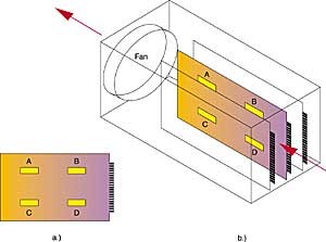
fig. 4. measurement of fan efficiency using bits.
after powering the board we waited until a thermal equilibrium had been reached. measurement could then be commenced. the fan was then switched on in the time interval between 150 and 790 sec. the resulting temperature measurements are plotted in fig.5, so allowing the cooling effect of the fan to be evaluated.
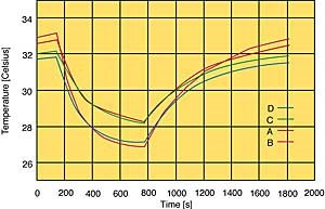
fig. 5. effect of the fan activity on the internal chip temperatures
(chip a=red, b=magenta, c=green, d=blue).
if the pcbs are built with packages equipped with bits circuitry a number of experimental investigations can be readily undertaken, e.g. the optimization of fan placement, checking the effect of vertical vs. horizontal card position, etc.
the integrity of the chip-to-ambient heat-removal path is very important when reliability issues are taken into account. small degradations in the heat conduction may result in higher operating temperature, which has a detrimental effect on reliability. an increase in the thermal resistance may indicate the start of a degradation process, e.g. die attach delamination, defects in the contact between the package and the cooling fins, etc.
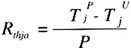
steady-state heat removal properties are usually characterized by the rthja thermal resistance:
rthja = (tj - ta) / p
where tj is the junction temperature, ta is the ambient temperature and p is the dissipated power. similarly, the dynamic (transient) thermal properties of the package are characterized by the zthja(t) thermal step-function response or transient thermal resistance:
zthja (t) = (tj(t) - ta) / p0
where tj(t) is the junction temperature as the function of the time, p0 is the amplitude of a dissipation step-function.
these expressions hold a certain ambiguity in the case of an environment where other power sources are responsible for the rise in temperature. this is true of a pcb, when the temperature rise in a package is influenced by heat dissipation from other packages. these equations can be reformulated in order to avoid this problem,. e.g. for the static thermal resistance we may write:
where  is the chip temperature if the chip is powered, is the chip temperature if the chip is powered,  is the temperature if the chip is unpowered. this equation is identical to the former one as long as the non-linear effects of the heat transfer can be neglected. is the temperature if the chip is unpowered. this equation is identical to the former one as long as the non-linear effects of the heat transfer can be neglected.
the bits circuit discussed earlier provides an easier way to measure "in-situ" the heat removing properties of the package. both the steady state and the transient thermal resistance can be measured if the chip is equipped with the bits circuitry. measurement of the and chip temperatures can be performed by using the built-in cmos sensor and the bs path.
a transient thermal resistance function is presented in fig.6. the chip was equipped with bits circuit accessible via bs path. the chip was mounted in a 48 pin ceramic dil package; the package was soldered into a pcb and was measured in natural convection. powering was realized by changing the digital control of the core circuit. the response was measured via the bs path. the asymptotic value of the function gives the static thermal resistance, which is about 44 k/w in this case.
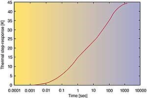
fig. 6. transient thermal resistance of a ceramic dil package,
measured through the bs path.
measurements can be made 'in-situ' which ultimately tells us much about the conditions of heat removal. if the used components incorporate bits and bitt circuitry the thermal features of all packages can be thoroughly tested, both on the production line and in the field. this test does not require any special equipment and may be performed using software.
the built-in thermal tester circuitry is also suitable for analyzing complex thermal effects, e.g. the thermal couplings between the neighboring packages of the pcb. if the bitt circuitry is controlled in such a way that the ps dissipation of a single selected package is switched on while thetk temperature rise of the other packages is measured, the coupling factors can be calculated between the one selected and the other packages under consideration.
conclusions
the paper describes a consistent set of hardware extensions proposed for digital vlsi circuits providing good thermal testability both at component and pcb level. these extensions include the built-in temperature sensor (bits), the built-in power switch and their interface to the boundary scan test circuit. if all these elements are incorporated, the chip is in effect equipped with the in-built thermal tester (bitt).
the advantages provided by the bitt are:
- on-line thermal monitoring at the pcb or system level
- measurement of the temperature very close to the hottest region (namely, the surface of the silicon chip)
- support for experimental investigation of cooling at chassis level (fan efficiency, dependencies on the pcb placement, etc.),
- support for static and transient thermal resistance measurements both in production and in the field
- measurement of the thermal coupling effects at the pcb level.
for a 20-25mm2 chip, the area required for the bitt circuit is less than 1%. this is more than compensated for by such benefits as better thermal management and the possibility of precise thermal measurements without the need for expensive dedicated equipment. this design for thermal testability approach is highly advisable for asics and other ics if the design is thermally stressed and reliability issues are of primary concern.
v. szekely
department of electron devices
technical university of budapest
|


